- | National Project |
Promoter |
Support Member |
TA/RA |
Research Team |
 Fusion Cafe |
Event & Schedule |
Conference |
Fusion Cafe |
Event & Schedule |
Conference |
Research Topics | | NUT | 文部科学省 | Home |
Support member
olecular Beam Epitaxy of Mn-doped IV, III-V, & II-IV-V2 Semiconductors Related Materials & Devices for Possible Spintronics Applications
名前と所属

Joel T. Asubar(ジョエル) H21〜H22.3.31 略歴:
1995 BSECE Mapua Institute of Technology
1996 Faculty Member Mapua Institute of Technology
1998 Master of Engineering (Electronics) Mapua Institute of Technology
1998 Design Engineer ROHM LSI Design
2001 Research Trainee Hitachi Central Research Laboratory
2006 Masters in Electronics, Electrical and Information Engineering
Nagaoka University of Technology
2009 Doctor in Information Science and Control Engineering
Nagaoka University of Technology
研究内容
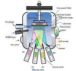
MBE
Epitaxial films grown by Molecular Beam Epitaxy (MBE) form the basis for today`s most advanced device structures in solid-state physics. MBE is an ultra high vacuum (∼10-10 Torr, translating to several hundreds of kms of atomic mean free path which is a few hundred thousand times the atomic diameter) non-equilibrium growth technique capable of predictability and reproducibly yielding materials with high degree of compositional and dimensional precision. It is the non-equilibrium growth aspect of MBE that makes it possible to prepare novel semiconductors such Mn-doped ZnSnAs2 epitaxial films.
ZnSnAs2
ZnSnAs2 is a member of the II-IV-V2 pnictide family of semiconductors which has attracted a great deal of interest since they exhibit properties with possible novel applications in the areas of visible and infrared LEDs and LASERs, infrared detectors, optical parametric oscillators, up-converters, and far infrared generation. Its being nearly-lattice matched with InP facilitates the integration with InP-based semiconductor devices such as LASERs, optical switches and detectors. Fig. 2 shows a high-resolution transmission electron microscopy (HR-TEM) image of a nearly lattice-matched p-ZnSnAs2/n-InP hetero-junction prepared in our MBE laboratory.
Diluted Magnetic Semiconductors
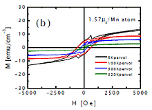
As it turns out from Dirac’s relativistic equation using quantum mechanics, the electron spins up or down while revolving around the nucleus. Spin, therefore, can effectively represent the binary logic “zero” and “one” and as such can represent information. The electron spin degree of freedom can be utilized in normally diamagnetic semiconductors by introducing magnetic transition atoms into the host semiconductor matrix. Such compounds are known as diluted magnetic semiconductors (DMS). In our laboratory, we have been preparing Mn-doped IV [JCG 311 (2009) 937], III-V [JCG 311 (2009) 933], and II-IV-V2 [JCG 311 (2009) 929] DMSs. We have also reported the first observed room temperature magnetism in Mn-doped ZnSnAs2 epitaxial films on nearly lattice-matched InP substrates [JCG 301-302 (2007) 656].
 |
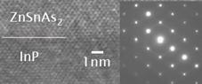 |
Fig. 1. Simplified drawing of the MBE growth chamber. |
Fig. 2 High-resolution TEM and TED images around the ZnSnAs2 - InP substrate interface [IEEE IPRM09, 255-258]. |
 |
|
| Fig. 3. The net M-H response of the Mn-doped ZnSnAs2 epitaxial films at 5K, 100K, 300K and 320K obtained by SQUID. |